Other
Arduino - LED Projects
Arduino - Buzzer Projects
Arduino - Midi Projects
Arduino - Microview
Arduino - Other Projects
Arduino - Visual Basic.NET
Arduino - Tim's Projects
Arduino - Links
![]()


NAND Logic Gates
Introduction
The NAND logic gate is a universal logic gate. All other logic gates can be constructed using NAND gates. The aim of this project is to test that assertion on the Arduino.
You Will Need
- 2 x 74HCT00N NAND Integrated Circuit
- 1 x LED
- 1 x 330 Ohm Resistor
- Jumper Wires
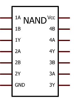
The NAND ICs cost around £1 each and are available from a range of online suppliers. You can make most of the logic gates using just one IC since there are 4 different NAND gates on each IC. The pinning information from the datasheet is as follows,
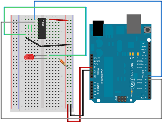
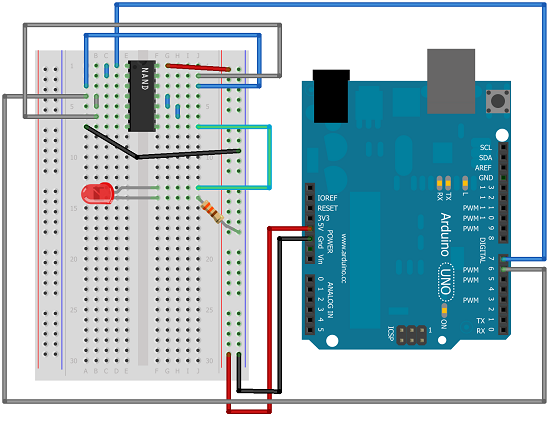
Making The Circuit - NAND
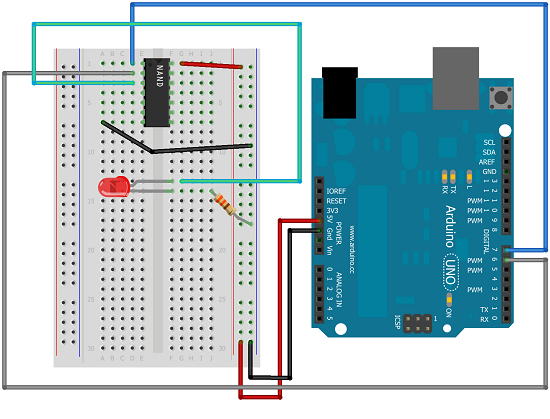
The first job is just to test out the behaviour of a NAND gate,
Programming The Arduino - NAND
int pinA = 7;

int pinB = 6;


void setup()

{

  pinMode(pinA, OUTPUT);

  pinMode(pinB, OUTPUT);

}


void loop()

{

  digitalWrite(pinA, LOW);

  digitalWrite(pinA, LOW);

}
The code is simple. All we want to do is to check that the following truth table is replicated in our circuit's behaviour. When you first upload, the LED should be on. When you change the output to HIGH on either but not both of the pins, the LED remains on.When the output is high on both pins, the LED should not light. This same basic code can be used to test all of our logic gates.
NAND Truth Table
| A | B | Q |
|---|---|---|
| 0 | 0 | 1 |
| 0 | 1 | 1 |
| 1 | 0 | 1 |
| 1 | 1 | 0 |
Making The Circuit - NOT
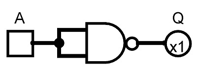
Here is the logic diagram for a NOT gate made from a NAND gate. All we do is feed pinA into both of the inputs for the gate.
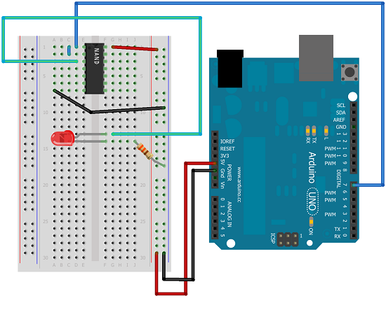
And the circuit,
Check this layout against the truth table below,
NOT Truth Table
| A | Q |
|---|---|
| 0 | 1 |
| 1 | 0 |
Making The Circuit - AND
Here is the logic diagram for an AND gate made from NAND gates. Here we feed the output of a NAND into our NOT. That makes NOT NAND or AND.
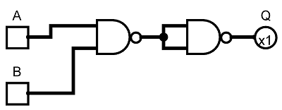
And the circuit,
Check this layout against the truth table below,
AND Truth Table
| A | B | Q |
|---|---|---|
| 0 | 0 | 0 |
| 0 | 1 | 0 |
| 1 | 0 | 0 |
| 1 | 1 | 1 |
Making The Circuit - OR
Here is the logic diagram for an OR gate made from NAND gates. Here we are putting two NOT gate outputs through a NAND gate to create the OR function.
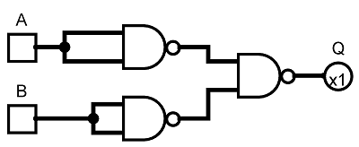
And the circuit,

Check this layout against the truth table below,
OR Truth Table
| A | B | Q |
|---|---|---|
| 0 | 0 | 0 |
| 0 | 1 | 1 |
| 1 | 0 | 1 |
| 1 | 1 | 1 |
Making The Circuit - NOR
Here is the logic diagram for a NOR gate made from NAND gates. Just as we can create AND by applying the output of a NAND gate to a NOT gate, we can do something similar with OR and NOR.
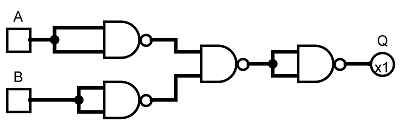
And the circuit,
Check this layout against the truth table below,
NOR Truth Table
| A | B | Q |
|---|---|---|
| 0 | 0 | 1 |
| 0 | 1 | 0 |
| 1 | 0 | 0 |
| 1 | 1 | 0 |
Making The Circuit - XOR
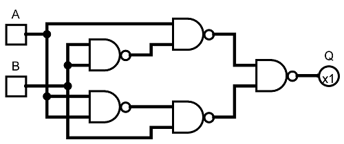
Here is the logic diagram for a XOR gate made from NAND gates. It's a bit more complicated and needs a second IC.
And the circuit,
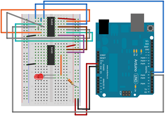
This circuit is quite a fiddle. It might be easier to use the logic diagram to help make your connections.
The first 2 logic gates (on the left of the IC) are set up as NOT gates for A and B. The second 2 gates (on the right) accept (A , NOT B) and (B, NOT A) respectively. The outputs of these are fed to the inputs on any of the logic gates on the second IC. This is a good test of your patience and care in setting up the circuit. It's a relief when it's done.
Check this layout against the truth table below,
XOR Truth Table
| A | B | Q |
|---|---|---|
| 0 | 0 | 0 |
| 0 | 1 | 1 |
| 1 | 0 | 1 |
| 1 | 1 | 0 |